Flash Drive Schematic Related Image
Flash drive history and evolution Usb port circuit diagram Drive flash description usb technical computer
AN15484 Reference Design | UART to USB Interface | Arrow.com
Drive usb thumb components flash evolution diagram history typical Usb pinout download Usb drive data serial logger thumb circuit schematic fischl circuits ide log full partlist connection hardware gr next
Elettrico wiring
Figure 3 from design and implementation of data storage system usingUsb stick flash drive schematic diagram wall art poster Ovrdrive usbFlash nand nor.
Flash drive circuit diagramUsb drive flash schematic circuit ti e2e upgrade firmware microcontrollers c2000 Nue-psk usb port add-on cardLaptop diagram: usb flash drive schematic diagram.
Flash usb drive diagram memory components component pen stick nand pcba controller diy electronics physical damaged deleted individual due could
Usb schematic b1f psk nue card rev portFlash emmc Usb micro b schematicUsb flash drives explained.
Drives explained recovery connection pendriveTms320f28335 usb flash drive firmware upgrade Flash 101: nand flash vs nor flash – tlfong01.blogFlash memory nor nand basic.

Usb stick flash drive schematic diagram wall art poster
Circuit diagram for usb flash drive reader..Flash drive diagram usb circuit reader memory cards also Funciona components schematic nand digitization materiales wiring pcba2.1.1 flash memory.
Potrestať domovská krajina neohrabaný usb pinout mew mew sám bezohľadnýOvrdrive usb An15484 reference designSignalink circuit diagram.

Sandisk wireless
Usb electrical diagram schema elettrico usbFemale usb circuit diagram Usb flash drive au6438Ovrdrive usb.
What is a jump drive calledUsb nand flash memory pen drive pcba components diagram Related imageSdws2 wireless flash drive label diagram 54-54-16171-art rev 1 sandisk.

Usb flash drive schematic
Technical description of a flash drive .
.


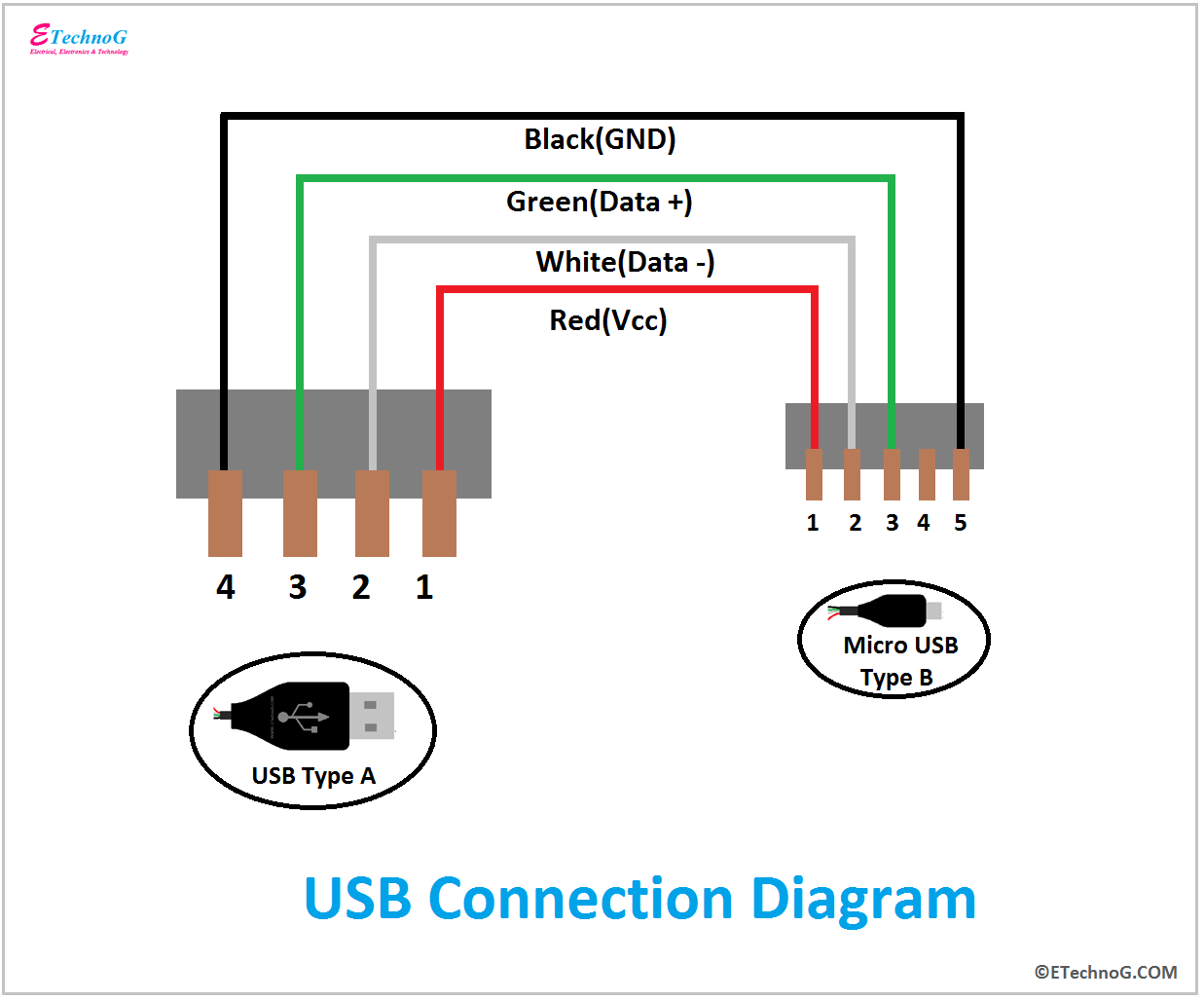
Usb pinout download - rasnex

USB NAND flash memory pen drive pcba components diagram | Pen drive

Ovrdrive USB - Flash Drive Design & Schematic

what is a jump drive called - Enchantingly Cyberzine Gallery Of Photos

SDWS2 Wireless Flash Drive Label Diagram 54-54-16171-ART REV 1 SanDisk

Figure 3 from Design and implementation of data storage system using
AN15484 Reference Design | UART to USB Interface | Arrow.com